RESEARCH ARTICLE

Ultrasensitive solar-blind ultraviolet detection and optoelectronic neuromorphic computing using α-In2Se3 phototransistors

  • Yuchen Cai 1,2 ,
  • Jia Yang 1,2 ,
  • Feng Wang , 1,2 ,
  • Shuhui Li 1,2 ,
  • Yanrong Wang 1,2 ,
  • Xueying Zhan 1,2 ,
  • Fengmei Wang 1,2 ,
  • Ruiqing Cheng , 3 ,
  • Zhenxing Wang , 1,2 ,
  • Jun He 3
Expand
  • 1. CAS Key Laboratory of Nanosystem and Hierarchical Fabrication, National Center for Nanoscience and Technology, Beijing 100190, China
  • 2. Center of Materials Science and Optoelectronics Engineering, University of Chinese Academy of Sciences, Beijing 100049, China
  • 3. Key Laboratory of Artificial Micro- and Nano-structures of Ministry of Education, School of Physics and Technology, Wuhan University, Wuhan 430072, China

Received date: 17 Oct 2022

Accepted date: 05 Dec 2022

Copyright

2023 Higher Education Press

Abstract

Detection of solar-blind ultraviolet (SB-UV) light is important in applications like confidential communication, flame detection, and missile warning system. However, the existing SB-UV photodetectors still show low sensitivities. In this work, we demonstrate the extraordinary SB-UV detection performance of α-In2Se3 phototransistors. Benefiting from the coupled semiconductor and ferroelectricity property, the phototransistor has an ultraweak detectable power of 17.85 fW, an ultrahigh gain of 1.2 × 10⁶, a responsivity of 2.6 × 10⁵ A/W, a detectivity of 1.3 × 10¹⁶ Jones and an ultralow noise-equivalent-power of 4.2 × 10⁻²⁰ W/Hz1/2 for 275 nm light. Its performance exceeds most other UV detectors, even including commercial photomultiplier tubes and avalanche photodiodes. It can be also implemented as an optoelectronic synapse for neuromorphic computing. A 784×300×10 artificial neural network (ANN) based on this optoelectronic synapse is constructed and demonstrated with a high recognition accuracy and good noise-tolerance for the Fashion-MNIST dataset. These extraordinary features endow this phototransistor with the potential for constructing advanced SB-UV detectors and intelligent hardware.

Cite this article

Yuchen Cai , Jia Yang , Feng Wang , Shuhui Li , Yanrong Wang , Xueying Zhan , Fengmei Wang , Ruiqing Cheng , Zhenxing Wang , Jun He . Ultrasensitive solar-blind ultraviolet detection and optoelectronic neuromorphic computing using α-In2Se3 phototransistors[J]. Frontiers of Physics, 2023 , 18(3) : 33308 . DOI: 10.1007/s11467-022-1241-7

1 Introduction

Because natural solar-blind ultraviolet (SB-UV) light with a wavelength of 200−300 nm is totally absorbed by the ozone layer, propagation of SB-UV signals loaded on artificial sources would not be disturbed on the earth’s surface. Therefore, the detection of SB-UV light facilitates applications including short-distance confidential communication, flame detection, missile warning systems, and so on [1-6]. Nevertheless, due to a severe attenuation during propagation, ultrasensitive SB-UV detectors with a high responsivity, a low noise-equivalent power (NEP), a high detectivity and a low dark current are lacking and highly demanded [7-12]. Different types of ultrasensitive detectors have been explored, but there still are non-negligible drawbacks. Commercial photomultiplier tubes (PMTs) are very sensitive but often severely constrained by their complicated structure, large size, and high energy consumption [13, 14]. Detectors based on normal p−n junctions, heterojunctions or Schottky diodes show huge potential in self-powered detection but often have poor figures of merit [5, 15-20]. Even though avalanche photodiodes (APDs) have an ultrahigh sensitivity even down to a single photon [21], the large voltage required for triggering an avalanche effect induces a high dark count rate and low energy efficiency.
Photoconductors based on some emerging semiconducting materials and their heterostructures have been demonstrated with high photoconductive gains and sensitivities, mainly due to the combination of a prolonged lifetime of majority and a short transit time [22-28]. With a simple device structure, these new-type photoconductors have a high potential for advanced SB-UV detectors. But this signal amplification mechanism usually leads to a slow response, a small bandwidth, and a high uncertainty. To address these problems, detectors based on ferroelectric semiconductor α-In2Se3 were explored very recently, where an ultrahigh gain induced by the light-induced polarization switching was found to endow the devices with ultrasensitive detection of even down to tens of photons [29]. Owing to the two-dimensional (2D) layered crystalline structure nature, an appropriate bandgap (1.38 eV) and a ferroelectric nature, α-In2Se3 also shows possibilities to construct new electronic and optoelectronic devices, including ultrasensitive SB-UV detectors.
In the meanwhile, neuromorphic analog computing based on synaptic devices has been studied for its high energy efficiency and parallel computation ability. Most synaptic devices are usually used in artificial neural networks (ANNs), connecting neurons with electrically programmable weights [30-35] and showing long-term plasticity, i.e., long-term potentiation (LTP) and long-term depression (LTD). Among these, memristors [36, 37], phase change memories [38], and 2D heterostructures [30, 34, 39] have been widely implemented for their extraordinary programmability. On the other hand, a series of optoelectronic memories have been also implemented whose conductance can be programmed by both optical and electrical pulses, which are often called optoelectronic synapses [32]. Even with good plasticity, most optoelectronic synapses still have low energy efficiency because of the strong light (radiant intensity over 0.1 mW/cm2) required for the weight modulations [30, 40-43]. Therefore, a more sensitive optoelectronic synapse is also demanded.
In this work, we demonstrate an α-In2Se3 phototransistor for ultrasensitive UV detection and neuromorphic computing. Benefiting from the inherent light-induced polarization switching mechanism in α-In2Se3, the phototransistor shows an ultrahigh sensitivity of 17.85 fW to SB-UV light. Moreover, this phototransistor has a fast response time of 400 μs, an ultrahigh responsivity of 2.6 × 10⁵ A/W, a high detectivity of 1.3 × 10¹⁶ Jones and an ultralow NEP of 4.2 × 10⁻²⁰ W/Hz1/2. Implemented as optoelectronic synapses in a 784 × 300 × 10 ANN, the phototransistor shows stable LTP and LTD behavior after being applied ultraweak optical pulses (0.003 mW/cm2) and identical gate electrical pulses respectively. When testing on a classification task, this ANN shows a high accuracy of 68.2% and a small degradation of 12% at a 50% noise level. These properties make this phototransistor a potential candidate for constructing advanced SB-UV photodetectors and optoelectronic synapses.

2 Methods

2.1 Device fabrications

Si wafers covered with 300 nm thick SiO2 were used as the substrates. The bottom gate of Cr/Au (8/30 nm) was patterned using electron beam lithography (EBL) and deposited using thermal vapor deposition. Then, HfO2 with a thickness of 25 nm was deposited as the gate insulator using atomic layer deposition (ALD). Then, mechanically exfoliated α-In2Se3 was transferred onto the stack using a standard wet-transfer method. Then, source and drain electrodes of Cr/Au (8/80 nm) were patterned and deposited. Lastly, a capping layer of 5 nm thick Al2O3 was deposited for encapsulation.

2.2 Electronic and optoelectronic measurements

Electronic and optoelectronic performances of the as-fabricated phototransistors were tested on a semiconductor analyzer system (Keysight B1500A). Temporal responses were collected with an LED source of 275 nm and a laser source of 360 nm. All tests were conducted under the condition of a high vacuum (<10−6 Torr) and a low temperature (~80 K). Illumination light powers were calibrated by a commercial photodiode power meter (Thorlabs, Inc.) and a commercial PMT photon-counter (Excelitas Technologies Corp.) (Supplementary Fig. S1).

2.3 Simulations

The ANN model was constructed and simulated on the CrossSim platform (webpage: cross-sim.sandia.gov). During the training process, synaptic weights of the ANN were updated following a backpropagation logarithm according to the LTP/LTD behavior experimentally tested. A standard image dataset (namely F-MNIST) containing 60000 images of 10 classes was used to train and test the constructed ANN.

3 Results

3.1 Basic characterizations

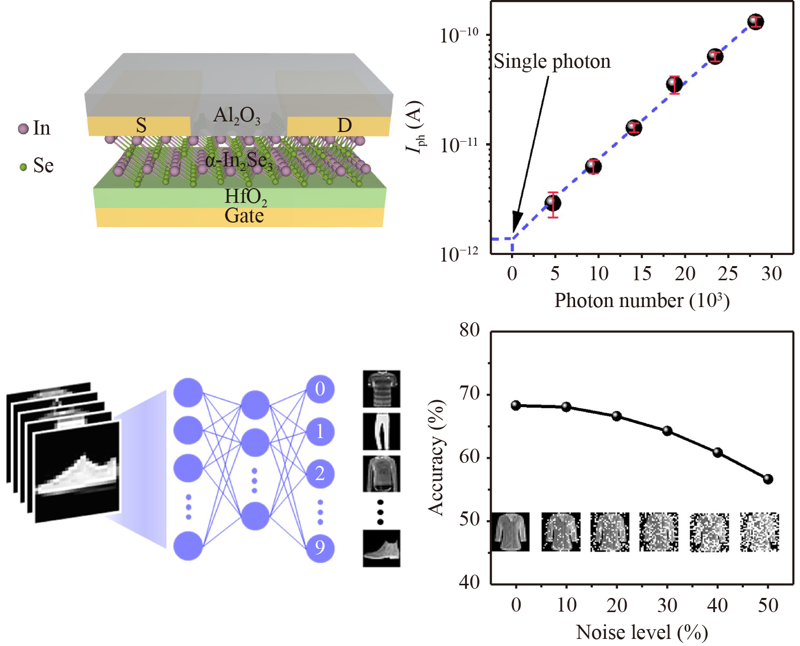
The schematic structure of the α-In2Se3 phototransistor is shown in Fig.1(a). High-k HfO2 was selected as the gate dielectric hence only a small gate voltage is needed for the electrical operations [44]. And apart from preventing contaminants from the environment, the top Al2O3 layer can induce an electron doping effect and strengthen the n-type semiconducting characteristic of the channel α-In2Se3 (Supplementary Fig. S2). After the fabrication process, the Raman spectrum of the channel was tested. As shown in Fig.1(b), peaks observed at 104, 181 and 193 cm−1 are corresponding to the A11, E4 and A31 modes of α-In2Se3 respectively, which is consistent with previous results [45, 46]. This demonstrates the high crystalline quality of the channel material after device fabrication.
Fig.1 Structure, characterizations and temporal response of the α-In2Se3 phototransistor. (a) Achematic structure of the α-In2Se3 phototransistor. S: Source; D: Drain. (b) Raman spectrum of the channel α-In2Se3. The inset shows an optical microscope image of the phototransistor. Scale bar: 3 μm. (c) Amplitude (blue) and phase (red) profiles during local voltage sweeping using a PFM tip. The arrows denote the forward/backward sweeping directions. The inset shows the schematic experimental setup for the local voltage sweeping. (d) Temporal response of the phototransistor under electrical and optical pulses. The time regions with positive, negative gate pulses and UV light pulses applied are denoted in blue, green and purple respectively. VDS: 0.5 V. Wavelength: 275 nm.

Full size|PPT slide

As the channel of the phototransistor, α-In2Se3 is a kind of 2D layered ferroelectric semiconductor whose ferroelectricity originates from the broken symmetry of the in-layer quintuple Se−In−Se−In−Se where the displacement of middle Se atoms induces the polarization switching. And the ferroelectric polarization of α-In2Se3 can be decomposed into two strongly coupled components, in-plane and out-of-plane components. Even though both components can contribute to tuning the conductance of α-In2Se3-based transistors [47], the out-of-plane polarization component is mainly in our consideration because it contributes to the most channel conductance under a small drain voltage [48-51], which can be proved by the no-hysteresis double-sweep output curve compared to a double-sweep transfer curve with a large hysteresis window (Supplementary Fig. S3). To confirm the ferroelectricity of the exfoliated α-In2Se3, a local voltage sweeping using a piezoelectric force microscope (PFM) tip was conducted and the amplitude and phase signals were collected. As shown in Fig.1(c), an obvious hysteresis in phase with a 180° reversal and a butterfly-like curve of amplitude can be observed, which validates the ferroelectric nature of α-In2Se3 [52].
As a ferroelectric semiconductor, α-In2Se3 shows two unusual features. The first is that its conductance states are strongly correlated with the ferroelectric polarization directions. Due to the accumulation/depletion of electrons at the α-In2Se3/gate dielectric interface, transistors based on α-In2Se3 have a nonvolatile low-resistance/high-resistance state (LRS/HRS) for ferroelectric polarization down/up state [53]. The second is that, because of the suitable bandgap and the existence of an imprint effect, light can flip the ferroelectricity of α-In2Se3 into a polarization down state, hence a nonvolatile LRS [29, 54, 55]. A brief band diagram analysis can be seen in Supplementary Fig. S4. In total, the conductance of the α-In2Se3 phototransistor can be repeatedly switched by electricity and light. This can be seen from the temporal response of an α-In2Se3 phototransistor to electrical and optical pulses as shown in Fig.1(d). The phototransistor was initially at an LRS with a large drain current of 0.11 μA. Then, an 8 V gate pulse (VGS) was applied at 1−2 s, setting the phototransistor into a polarization-up state and HRS. And a following −9 V gate pulse at 3−4 s can set it back to a polarization down state and LRS. Similar conductance switching can be also observed using electrical and UV light pulses, where an LRS can be achieved after being applied a 275 nm UV light pulse at 7−8 s. A retention time of over 10000 s can be achieved both at LRS and HRS (see Supplementary Fig. S5).

3.2 Photodetection performance

UV detection performance of the phototransistor was investigated by testing its temporal responses to lights with various intensities and wavelengths. Before light illumination, the phototransistor was set into an HRS with a very low dark current of below 0.3 pA using a positive gate pulse and this low dark current can be very stable with a long retention time of over 10000 s (Supplementary Fig. S6). As shown in Fig.2(a), temporal response under 5 cycles of alternating optical and electrical pulses were collected. In each period, 275 nm SB-UV lights with different power intensities were applied for 5 seconds. Note that the active powers are the multiplications of the incident power densities and the device channel area (30 μm2). The weakest power used is 17.85 fW, much weaker than most exiting SB-UV photodetectors (as will be discussed later). A cycle test of a 360 nm light was also conducted with the weakest power of 0.57 fW (Supplementary Fig. S7), showing the sub-fW level sensitivity of the detector at a longer wavelength. In response to UV light, the rise time can be as fast as 400 μs, and a 50 ns gate pulse can be applied to reset the detector to the initial HRS (Supplementary Figs. S8 and S9). One possible reason for the difference between these two values is that the gate voltage can induce a global electric field in the α-In2Se3 channel which facilitates fast reversed-domain nucleation and growth [56], while a light-induced switching process is constrained by the carrier generation and migration process.
Fig.2 UV detection performance of the α-In2Se3 phototransistor. (a) Temporal response under 5 cycles of alternating optical and electrical pulses with a period of 20 s. Optical pulse: width 5 s, amplitude varying from 17.85 fW to 22.84 pW. Gate electrical pulse: width 1 s, amplitude 4 V. VDS: 1 V. (b) Responsivity and (c) NEP dependent on power at 275 nm and 360 nm. (d) Photocurrent dependent on incident photon number. The dashed line through data points is a linear fit of the points with error bars. Photocurrent at a single photon is extrapolated to be 1.4 pA. Comparison of (e) responsivity and (f) NEP among various types of UV detectors. Data sources of PMT and APD are collected from commercial products: PMTSS and APD430A2 (Thorlabs, Inc.). The detailed information is listed in Supplementary Table 1.

Full size|PPT slide

Responsivity (Rph) is a basic figure of merit for a photodetector, which is defined by Rph = Iph/Pin, where Iph is photocurrent and Pin is the power of incident light received by the detector. Owing to the ultra-low dark current at the HRS and the large current gain during light illumination, Iph is approximately equal to the current after illumination. As shown in Fig.2(b), responsivity achieves a maximum value at a threshold power Pth. And Pth is equal to 0.23 pW for 275 nm and 1.96 fW for 360 nm. The maximum responsivity is 2.6 × 10⁵ A/W and 4.5 × 10⁶ A/W for 275 nm and 360 nm, respectively. The ultrahigh responsivity originates from the high gain (G), which is defined as G = hcRph/(), where h is Planck’s constant, c is the velocity of light, e is the electron charge and λ is the wavelength. The calculated gain of the phototransistor reaches 1.6×10⁷ at most [Supplementary Fig. S10(a)], which is comparable to commercial photon-number-resolved detectors like avalanche photodiodes (APDs) and photomultipliers (PMTs) (between 104 to 1010) [57]. The high gain results from the high efficiency of the light-induced polarization switching process, which induces a giant current change under weak light illumination due to the ferroelectric polarization-related conducting effect.
A low noise current (in) is important for sensitive photodetectors. Here, by fitting the noise spectrum [Supplementary Fig. S10(b)], an overall noise current of below 0.1 pA/Hz1/2 can be obtained, which is very low compared to other detectors. Combining noise current and responsivity, noise-equivalent power (NEP) can be calculated by
NEP=in2Rph,
where in2 is the root-mean-squared noise current over all frequencies. NEP tells the minimum incident light power that can be recognized out. Because of the low noise current and ultrahigh responsivity, the overall NEP of the device is below 2 × 10⁻¹⁷ W/Hz1/2, achieves 4.2 × 10⁻²⁰ W/Hz1/2 at 275 nm and the lowest value of 2.4 × 10⁻²¹ W/Hz1/2 at 360 nm [Fig.2(c)]. Detectivity is usually a comprehensive figure of merit for photodetectors and is defined as
D*=AΔfNEP,
where A is the device active area and Δf is the bandwidth. Detectivity of the phototransistor can reach 1.3 × 10¹⁶ Jones at 275 nm and 2.3 × 10¹⁷ Jones at 360 nm (Supplementary Fig. S10(c)). The repeatability of the above figures of merit was validated on another device (Supplementary Fig. S11).
The sensitivity of this detector can achieve a higher level when it is set to a photon-counting mode, similar to the Geiger mode of APDs. Fig.2(d) shows the dependence of photocurrent on photon number. We see the photocurrent is exponentially related to the number of incident photons within a tolerable error range. And the device can distinguish photon numbers as low as 5000. In addition, the extrapolated photocurrent at the single photon (1.4 pA) exceeds the dark current (~0.3 pA), indicating that it is possible to achieve a photon-number resolution by using more accurate readout circuits and single-photon sources. Commercial PMTs and APDs are very sensitive as well but are usually limited by the large size and high operating voltage. While our phototransistor may address these problems due to its low operating voltage (<5 V) and the ability to be freely integrated with Si or other 2D materials by van der Waals integration, and the dielectric layer HfO2 can also be replaced by other oxides like SiO2 or Al2O3 (see Supplementary Fig. S12), which endows the device with a wider application range.
To sum up the overall performance of the phototransistor as a UV detector, comparisons among this phototransistor and other previously reported UV detectors are shown in Fig.2(e) and (f). In contrast to other types of prevailing UV detectors, especially SB-UV detectors (GaN, h-BN), narrow-bandgap detectors (Te, BP), and commercial products (PMTs and APDs), the α-In2Se3 phototransistor has the highest responsivity and the lowest NEP. It is also worth noting that our device has the weakest detectable power, which further proves its huge potential for ultrasensitive UV detection.

3.3 Neuromorphic computing

In brains of human beings, neurons are interconnected by numerous synapses, through which active signals are transported from one neuron to other neurons. During signal transportation, connection strengths, i.e., weights of synapses, can be tuned flexibly to realize a learning process. This behavior of synapses is called long-term plasticity, including long-term potentiation (LTP) and long-term depression (LTD). Inspired by this, our phototransistor can be implemented as an optoelectronic “synapse” in artificial neural networks (ANNs), because its conductance state can be tuned as the weight with electrical or optical signals.
As shown in Fig.3(a), we demonstrate LTP and LTD serially for 19 cycles. In each LTP-LTD weight modulation process, we adopted an identical pulse scheme, where 100 1 ms-width optical pulses and subsequent 100 1 ms-width gate electrical pulses were applied on the synapse with a fixed pulse interval of 50 ms. After each optical/electrical pulse, the synapse is changed to a new conductance state and kept stable until the next pulse comes. Note that the optical pulses have an amplitude of about 1 pW, corresponding to a radiant intensity of 0.003 mW/cm2, which is very weaker compared to that of most other optoelectronic synapses [30, 40-43]. After successfully demonstrating LTP and LTD on a single device, we conducted an α-In2Se3 phototransistor-based ANN via simulation. We constructed an ANN containing 784 × 300 × 10 full-connected three-layer neurons [as illustrated in Fig.3(b)] on the CrossSim platform (the details can be seen in Section 2). The experimentally collected LTP and LTD were used as guidance for weight updating during the training process. The input neurons receive grayscale values of pixels in one input image at one time and they are transferred through weighted artificial synapses to the hidden layer and ultimately to the output layer. The ultimate scores in 10 output neurons decide the recognized class of the input images.
Fig.3 Demonstration of the α-In2Se3 phototransistor as an optoelectronic synapse in an ANN. (a) Pulse-dependent LTP and LTD behaviors of the synapse. During each conductance increasing/decreasing period, 100 optical/electrical pulses with a width of 1 ms and an amplitude of 1 pW/1 V were periodically applied with a period of 50 ms. (b) Schematic illustration of the 784×300×10 ANN used for an image classification task. The input images are from the F-MNIST dataset and the 10 output digits represent 10 classes of objects. (c) Recognition accuracy evolves as a function of training epoch with a dataset noise level varying from zero to 50%. (d) The final recognition accuracy (after 15 training epochs) as a function of the noise level. The inset shows typical images with different noise levels.

Full size|PPT slide

Finally, its performance on the Fashion-MNIST (F-MNIST) dataset with different noise levels was calculated and evaluated [58]. Recognition accuracy evolving during the training process at different noise levels was computed and the results are shown in Fig.3(c). After 15 training epochs, recognition accuracy reaches 68.2% without noise and can still achieve 56.6% even with a 50% noise level, as shown in Fig.3(d). These results validate the feasibility of implementing the phototransistor as an optoelectronic synapse. And it also can be implemented as a pure-electric synapse with pure-electric LTP/LTD behaviors, which further endows it with a wider application range in neuromorphic computing (Supplementary Fig. S13).

4 Conclusion

In summary, we fabricate an α-In2Se3 phototransistor and demonstrate its extraordinary UV detection performance and potential as an optoelectronic synapse for constructing neuromorphic computing hardware. As an SB-UV (275 nm) detector, the phototransistor has an ultraweak detectable power of 17.85 fW, a response time of 400 μs, an ultrahigh gain of 1.2 × 10⁶, a responsivity of 2.6 × 10⁵ A/W, a detectivity of 1.3 × 10¹⁶ Jones and an ultralow NEP of 4.2 × 10⁻²⁰ W/Hz1/2. At a longer wavelength (360 nm), its minimum detectable power and NEP can be decreased to 0.57 fW and 2.4 × 10⁻²¹ W/Hz1/2 respectively, responsivity and detectivity can be promoted to 4.5 × 10⁶ A/W and 2.3 × 10¹⁷ Jones respectively. These figures of merits are the best among various UV detectors. Moreover, working in a photon-counting mode, as low as 5000 photons can be distinguished and a photon-number resolution might be realized. We further implement the device as an artificial optoelectronic synapse for neuromorphic computing. The device shows LTP and LTD behavior when being applied identical optical pulses and gate electrical pulses. With optically/electrically alterable conductance, the phototransistor is used to construct a 784 × 300 × 10 artificial neural network for image recognition. After being trained for 15 epochs, the accuracy can achieve 68.2% when recognizing F-MNIST images without noise, and just decreased by 12% even with a 50% noise, showing a good noise-tolerance.

Electronic Supplementary Material

The online version contains supplementary material available at https://doi.org/10.1007/10.1007/s11467-022-1241-7 and https://journal.hep.com.cn/fop/EN/10.1007/s11467-022-1241-7.

Acknowledgements

This work was supported by the National Key R&D Program of China (Grant Nos. 2021YFA1201500 and 2018YFA0703700), the National Natural Science Foundation of China (Nos. 91964203, 61974036, 62274046, 22179029, and 12204122), the Strategic Priority Research Program of Chinese Academy of Sciences (Nos. XDB44000000), the Fundamental Research Funds for the Central Universities (No. 2042021kf0067), and CAS Key Laboratory of Nanosystem and Hierarchical Fabrication. The authors also gratefully acknowledge the support of Youth Innovation Promotion Association CAS.
1
M. Gong , Q. Liu , B. Cook , B. Kattel , T. Wang , W. L. Chan , D. Ewing , M. Casper , A. Stramel , J. Z. Wu . All-printable ZnO quantum dots/graphene van der Waals heterostructures for ultrasensitive detection of ultraviolet light. ACS Nano, 2017, 11(4): 4114

DOI

2
X.XuJ.ChenS.CaiZ.LongY.ZhangL.SuS.HeC.TangP.LiuH.PengX.Fang, A real-time wearable UV-radiation monitor based on a high-performance p-CuZnS/n-TiO2 photodetector, Adv. Mater. 30(43), 1803165 (2018)

3
D. Zhang , W. Zheng , R. Lin , Y. Li , F. Huang . Ultrahigh EQE (15%) solar‐blind UV photovoltaic detector with organic–inorganic heterojunction via dual built‐in fields enhanced photogenerated carrier separation efficiency mechanism. Adv. Funct. Mater., 2019, 29(26): 1900935

DOI

4
C. N. Lin , Y. J. Lu , X. Yang , Y. Z. Tian , C. J. Gao , J. L. Sun , L. Dong , F. Zhong , W. D. Hu , C. X. Shan . Diamond-based all-carbon photodetectors for solar-blind imaging. Adv. Opt. Mater., 2018, 6(15): 1800068

DOI

5
W. Yang , K. Hu , F. Teng , J. Weng , Y. Zhang , X. Fang . High-performance silicon-compatible large-area UV-to-visible broadband photodetector based on integrated lattice-matched Type II Se/n-Si heterojunctions. Nano Lett., 2018, 18(8): 4697

DOI

6
Y. Zhang , S. Li , Z. Li , H. Liu , X. Liu , J. Chen , X. Fang . High-performance two-dimensional perovskite Ca2Nb3O10 UV photodetectors. Nano Lett., 2021, 21(1): 382

DOI

7
A. Kumar , M. A. Khan , M. Kumar . Recent advances in UV photodetectors based on 2D materials: A review. J. Phys. D Appl. Phys., 2022, 55(13): 133002

DOI

8
R. Cao , Y. Zhang , H. Wang , Y. Zeng , J. Zhao , L. Zhang , J. Li , F. Meng , Z. Shi , D. Fan , Z. Guo . Solar-blind deep-ultraviolet photodetectors based on solution-synthesized quasi-2D Te nanosheets. Nanophotonics, 2020, 9(8): 2459

DOI

9
W. Zheng , R. Lin , Z. Zhang , F. Huang . Vacuum-ultraviolet photodetection in few-layered h-BN. ACS Appl. Mater. Interfaces, 2018, 10(32): 27116

DOI

10
J. Chu , F. Wang , L. Yin , L. Lei , C. Yan , F. Wang , Y. Wen , Z. Wang , C. Jiang , L. Feng , J. Xiong , Y. Li , J. He . High-performance ultraviolet photodetector based on a few-layered 2D NiPS3 nanosheet. Adv. Funct. Mater., 2017, 27(32): 1701342

DOI

11
W. Y. Kong , G. A. Wu , K. Y. Wang , T. F. Zhang , Y. F. Zou , D. D. Wang , L. B. Luo . Graphene-β-Ga2O3 heterojunction for highly sensitive deep UV photodetector application. Adv. Mater., 2016, 28(48): 10725

DOI

12
S. Li , Y. Zhang , W. Yang , H. Liu , X. Fang . 2D perovskite Sr2Nb3O10 for high‐performance UV photodetectors. Adv. Mater., 2020, 32(7): 1905443

DOI

13
B. K. Lubsandorzhiev . On the history of photomultiplier tube invention. Nucl. Instrum. Methods Phys. Res. A, 2006, 567(1): 236

DOI

14
A. Lafuente , A. Abanades , P. T. Leon , F. Sordo , J. M. Martinez-Val . Dynamic response of an accelerator driven system to accelerator beam interruptions for criticality. Nucl. Instrum. Methods Phys. Res. A, 2008, 591(2): 327

DOI

15
L. Su , Q. Zhang , T. Wu , M. Chen , Y. Su , Y. Zhu , R. Xiang , X. Gui , Z. Tang . High-performance zero-bias ultraviolet photodetector based on p-GaN/n-ZnO heterojunction. Appl. Phys. Lett., 2014, 105(7): 072106

DOI

16
B. Nie , J. G. Hu , L. B. Luo , C. Xie , L. H. Zeng , P. Lv , F. Z. Li , J. S. Jie , M. Feng , C. Y. Wu , Y. Q. Yu , S. H. Yu . Monolayer graphene film on ZnO nanorod array for high-performance Schottky junction ultraviolet photodetectors. Small, 2013, 9(17): 2872

DOI

17
X. Wan , Y. Xu , H. Guo , K. Shehzad , A. Ali , Y. Liu , J. Yang , D. Dai , C. T. Lin , L. Liu , H. C. Cheng , F. Wang , X. Wang , H. Lu , W. Hu , X. Pi , Y. Dan , J. Luo , T. Hasan , X. Duan , X. Li , J. Xu , D. Yang , T. Ren , B. Yu . A self-powered high-performance graphene/silicon ultraviolet photodetector with ultra-shallow junction: Breaking the limit of silicon?. npj 2D Mater. Appl., 2017, 1(1): 4

DOI

18
M. A. Kang , S. Kim , I. S. Jeon , Y. R. Lim , C. Y. Park , W. Song , S. S. Lee , J. Lim , K. S. An , S. Myung . Highly efficient and flexible photodetector based on MoS2–ZnO heterostructures. RSC Adv., 2019, 9(34): 19707

DOI

19
H. Li , S. Su , C. Liang , M. Huang , X. Ma , G. Yu , H. Tao . Ultraviolet photodetector based on the hybrid graphene/phosphor field-effect transistor. Opt. Mater., 2020, 109: 110439

DOI

20
V. Krishnamurthi , M. X. Low , S. Kuriakose , S. Sriram , M. Bhaskaran , S. Walia . Black phosphorus nanoflakes vertically stacked on MoS2 nanoflakes as heterostructures for photodetection. ACS Appl. Nano Mater., 2021, 4(7): 6928

DOI

21
J. Seo , J. H. Lee , J. Pak , K. Cho , J. K. Kim , J. Kim , J. Jang , H. Ahn , S. C. Lim , S. Chung , K. Kang , T. Lee . Ultrasensitive photodetection in MoS2 avalanche phototransistors. Adv. Sci. (Weinh.), 2021, 8(19): 2102437

DOI

22
V. Adinolfi , E. H. Sargent . Photovoltage field-effect transistors. Nature, 2017, 542(7641): 324

DOI

23
F. P. García de Arquer , A. Armin , P. Meredith , E. H. Sargent . Solution-processed semiconductors for next-generation photodetectors. Nat. Rev. Mater., 2017, 2(3): 16100

DOI

24
J. Feng , C. Gong , H. Gao , W. Wen , Y. Gong , X. Jiang , B. Zhang , Y. Wu , Y. Wu , H. Fu , L. Jiang , X. Zhang . Single-crystalline layered metal-halide perovskite nanowires for ultrasensitive photodetectors. Nat. Electron., 2018, 1(7): 404

DOI

25
X. Gong , M. Tong , Y. Xia , W. Cai , J. S. Moon , Y. Cao , G. Yu , C. L. Shieh , B. Nilsson , A. J. Heeger . High-detectivity polymer photodetectors with spectral response from 300 nm to 1450 nm. Science, 2009, 325(5948): 1665

DOI

26
G. Konstantatos , M. Badioli , L. Gaudreau , J. Osmond , M. Bernechea , F. P. Garcia de Arquer , F. Gatti , F. H. Koppens . Hybrid graphene-quantum dot phototransistors with ultrahigh gain. Nat. Nanotechnol., 2012, 7(6): 363

DOI

27
F. Guo , B. Yang , Y. Yuan , Z. Xiao , Q. Dong , Y. Bi , J. Huang . A nanocomposite ultraviolet photodetector based on interfacial trap-controlled charge injection. Nat. Nanotechnol., 2012, 7(12): 798

DOI

28
Y. Zhang , D. J. Hellebusch , N. D. Bronstein , C. Ko , D. F. Ogletree , M. Salmeron , A. P. Alivisatos . Ultrasensitive photodetectors exploiting electrostatic trapping and percolation transport. Nat. Commun., 2016, 7(1): 11924

DOI

29
J. Yang , F. Wang , J. F. Guo , Y. R. Wang , C. X. Jiang , S. H. Li , Y. C. Cai , X. Y. Zhan , X. F. Liu , Z. H. Cheng , J. He , Z. X. Wang . Ultrasensitive ferroelectric semiconductor phototransistors for photon‐level detection. Adv. Funct. Mater., 2022, 32(36): 2205468

DOI

30
Y. X. Hou , Y. Li , Z. C. Zhang , J. Q. Li , D. H. Qi , X. D. Chen , J. J. Wang , B. W. Yao , M. X. Yu , T. B. Lu , J. Zhang . Large-scale and flexible optical synapses for neuromorphic computing and integrated visible information sensing memory processing. ACS Nano, 2021, 15(1): 1497

DOI

31
E. J. Fuller , F. E. Gabaly , F. Leonard , S. Agarwal , S. J. Plimpton , R. B. Jacobs-Gedrim , C. D. James , M. J. Marinella , A. A. Talin . Li-ion synaptic transistor for low power analog computing. Adv. Mater., 2017, 29(4): 1604310

DOI

32
J. Sun , S. Oh , Y. Choi , S. Seo , M. J. Oh , M. Lee , W. B. Lee , P. J. Yoo , J. H. Cho , J. H. Park . Optoelectronic synapse based on IGZO-alkylated graphene oxide hybrid structure. Adv. Funct. Mater., 2018, 28(47): 1804397

DOI

33
Z. Luo , Z. Wang , Z. Guan , C. Ma , L. Zhao , C. Liu , H. Sun , H. Wang , Y. Lin , X. Jin , Y. Yin , X. Li . High-precision and linear weight updates by subnanosecond pulses in ferroelectric tunnel junction for neuro-inspired computing. Nat. Commun., 2022, 13(1): 699

DOI

34
S. Wang , L. Liu , L. Gan , H. Chen , X. Hou , Y. Ding , S. Ma , D. W. Zhang , P. Zhou . Two-dimensional ferroelectric channel transistors integrating ultra-fast memory and neural computing. Nat. Commun., 2021, 12(1): 53

DOI

35
Y. van de Burgt , E. Lubberman , E. J. Fuller , S. T. Keene , G. C. Faria , S. Agarwal , M. J. Marinella , A. Alec Talin , A. Salleo . A non-volatile organic electrochemical device as a low-voltage artificial synapse for neuromorphic computing. Nat. Mater., 2017, 16(4): 414

DOI

36
M. Prezioso , F. Merrikh-Bayat , B. D. Hoskins , G. C. Adam , K. K. Likharev , D. B. Strukov . Training and operation of an integrated neuromorphic network based on metal-oxide memristors. Nature, 2015, 521(7550): 61

DOI

37
D. B. Strukov , G. S. Snider , D. R. Stewart , R. S. Williams . The missing memristor found. Nature, 2008, 453(7191): 80

DOI

38
T. Tuma , A. Pantazi , M. Le Gallo , A. Sebastian , E. Eleftheriou . Stochastic phase-change neurons. Nat. Nanotechnol., 2016, 11(8): 693

DOI

39
C. Y. Wang , S. J. Liang , S. Wang , P. F. Wang , Z. A. Li , Z. R. Wang , A. Y. Gao , C. Pan , C. Liu , J. Liu , H. F. Yang , X. W. Liu , W. H. Song , C. Wang , B. Cheng , X. M. Wang , K. J. Chen , Z. L. Wang , K. J. Watanabe , T. Taniguchi , J. J. Yang , F. Miao . Gate-tunable van der Waals heterostructure for reconfigurable neural network vision sensor. Sci. Adv., 2020, 6(26): eaba6173

DOI

40
T. Ahmed , M. Tahir , M. X. Low , Y. Ren , S. A. Tawfik , E. L. H. Mayes , S. Kuriakose , S. Nawaz , M. J. S. Spencer , H. Chen , M. Bhaskaran , S. Sriram , S. Walia . Fully light-controlled memory and neuromorphic computation in layered black phosphorus. Adv. Mater., 2021, 33(10): 2004207

DOI

41
T. Y. Wang , J. L. Meng , Z. Y. He , L. Chen , H. Zhu , Q. Q. Sun , S. J. Ding , P. Zhou , D. W. Zhang . Ultralow power wearable heterosynapse with photoelectric synergistic modulation. Adv. Sci. (Weinh.), 2020, 7(8): 1903480

DOI

42
F. Zhou , Z. Zhou , J. Chen , T. H. Choy , J. Wang , N. Zhang , Z. Lin , S. Yu , J. Kang , H. P. Wong , Y. Chai . Optoelectronic resistive random access memory for neuromorphic vision sensors. Nat. Nanotechnol., 2019, 14(8): 776

DOI

43
Q. Wu , J. Wang , J. Cao , C. Lu , G. Yang , X. Shi , X. Chuai , Y. Gong , Y. Su , Y. Zhao , N. Lu , D. Geng , H. Wang , L. Li , M. Liu . Photoelectric plasticity in oxide thin film transistors with tunable synaptic functions. Adv. Electron. Mater., 2018, 4(12): 1800556

DOI

44
P. Luo , C. Liu , J. Lin , X. Duan , W. Zhang , C. Ma , Y. Lv , X. Zou , Y. Liu , F. Schwierz , W. Qin , L. Liao , J. He , X. Liu . Molybdenum disulfide transistors with enlarged van der Waals gaps at their dielectric interface via oxygen accumulation. Nat. Electron., 2022, 5(12): 849

DOI

45
J. Y. Yang , M. J. Yeom , Y. Park , J. Heo , G. Yoo . Ferroelectric α‐In2Se3 wrapped‐gate β‐Ga2O3 field‐effect transistors for dynamic threshold voltage control. Adv. Electron. Mater., 2021, 7(8): 2100306

DOI

46
J. Cui , L. Wang , Z. Du , P. Ying , Y. Deng . High thermoelectric performance of a defect in α-In2Se3-based solid solution upon substitution of Zn for In. J. Mater. Chem. C, 2015, 3(35): 9069

DOI

47
J. J. Wang , F. Wang , Z. X. Wang , W. H. Huang , Y. Y. Yao , Y. R. Wang , J. Yang , N. N. Li , L. Yin , R. Q. Cheng , X. Y. Zhan , C. X. Shan , J. He . Logic and in-memory computing achieved in a single ferroelectric semiconductor transistor. Sci. Bull. (Beijing), 2021, 66(22): 2288

DOI

48
W. Ding , J. Zhu , Z. Wang , Y. Gao , D. Xiao , Y. Gu , Z. Zhang , W. Zhu . Prediction of intrinsic two-dimensional ferroelectrics in In2Se3 and other III2-VI3 van der Waals materials. Nat. Commun., 2017, 8(1): 14956

DOI

49
Y. Zhou , D. Wu , Y. Zhu , Y. Cho , Q. He , X. Yang , K. Herrera , Z. Chu , Y. Han , M. C. Downer , H. Peng , K. Lai . Out-of-plane piezoelectricity and ferroelectricity in layered α-In2Se3 nanoflakes. Nano Lett., 2017, 17(9): 5508

DOI

50
F. Xue , W. Hu , K. C. Lee , L. S. Lu , J. Zhang , H. L. Tang , A. Han , W. T. Hsu , S. Tu , W. H. Chang , C. H. Lien , J. H. He , Z. Zhang , L. J. Li , X. Zhang . Room-temperature ferroelectricity in hexagonally layered α-In2Se3 nanoflakes down to the monolayer limit. Adv. Funct. Mater., 2018, 28(50): 1803738

DOI

51
C. Zheng , L. Yu , L. Zhu , J. L. Collins , D. Kim , Y. Lou , C. Xu , M. Li , Z. Wei , Y. Zhang , M. T. Edmonds , S. Li , J. Seidel , Y. Zhu , J. Z. Liu , W. X. Tang , M. S. Fuhrer . Room temperature in-plane ferroelectricity in van der Waals In2Se3. Sci. Adv., 2018, 4(7): eaar7720

DOI

52
Y. Zhang , L. Wang , H. Chen , T. Ma , X. Lu , K. P. Loh . Analog and digital mode α‐In2Se3 memristive devices for neuromorphic and memory applications. Adv. Electron. Mater., 2021, 7(12): 2100609

DOI

53
M. Si , A. K. Saha , S. Gao , G. Qiu , J. Qin , Y. Duan , J. Jian , C. Niu , H. Wang , W. Wu , S. K. Gupta , P. D. Ye . A ferroelectric semiconductor field-effect transistor. Nat. Electron., 2019, 2(12): 580

DOI

54
F. Xue , X. He , W. Liu , D. Periyanagounder , C. Zhang , M. Chen , C. H. Lin , L. Luo , E. Yengel , V. Tung , T. D. Anthopoulos , L. J. Li , J. H. He , X. Zhang . Optoelectronic ferroelectric domain‐wall memories made from a single van der Waals ferroelectric. Adv. Funct. Mater., 2020, 30(52): 2004206

DOI

55
K. Xu , W. Jiang , X. Gao , Z. Zhao , T. Low , W. Zhu . Optical control of ferroelectric switching and multifunctional devices based on van der Waals ferroelectric semiconductors. Nanoscale, 2020, 12(46): 23488

DOI

56
Y. Zhang , J. Dai , X. Zhong , D. Zhang , G. Zhong , J. Li . Probing ultrafast dynamics of ferroelectrics by time-resolved pump-probe spectroscopy. Adv. Sci. (Weinh.), 2021, 8(22): 2102488

DOI

57
H. Wang , J. Guo , J. Miao , W. Luo , Y. Gu , R. Xie , F. Wang , L. Zhang , P. Wang , W. Hu . Emerging single-photon detectors based on low-dimensional materials. Small, 2022, 18(5): 2103963

DOI

58
X.HanR.KashifV.Roland, Fashion-MNIST: A novel image dataset for benchmarking machine learning algorithms, arXiv: 1708.07747 (2017)

Outlines

/