

1 Introduction
Antimony selenide (Sb2Se3), a semiconductor possessing one dimensional crystal structure [1], is an excellent photovoltaic absorber due to its high absorption coefficient (>105 cm−1) at visible region [2], 1.17 eV band gap (optimal for single junction solar cells) [3], simple binary composition with fixed orthorhombic phase [4], low toxicity, and earth-abundant constituents. What’s more, theoretical calculation and experimental characterizations confirmed that Sb2Se3 has benign grain boundaries (GBs) if properly aligned along the ribbon direction [5]. In recent years, through steady improvements in the growth of these aligned Sb2Se3 films, power conversion efficiency (PCE) of Sb2Se3 thin film solar cells has increased to 5.6% [5–9], which is larger than other non-cubic semiconductor thin film solar cells such as SnS (reported best PCE of 4.6%) [10].
Despite the rapid improvement, the device efficiency is still far behind conventional copper indium gallium selenide (CIGS, PCE= 22.3%) [11], cadmium telluride (CdTe, PCE= 22.1%) [12], copper zinc tin sulfoselenide (CZTSSe, PCE= 12.6%) [13], and even amorphous silicon (PCE= 13.6%) solar cells [14]. One reason is that the fundamental features of thin film Sb2Se3 such as mobility, carrier lifetime, diffusion length, defect depth, defect density and optical band tails remain largely unexplored. Only film conductivity and carrier mobilities were reported in few previous studies [15,16]. The study on Sb2Se3 is lacking because of three difficulties: the intrinsically low electrical conductivity (10−6−10−7 S·cm−1) of Sb2Se3 film creates obstacles for obtaining carrier density and mobility directly from Hall effect measurement [17]; the absence of photoluminescence due to its indirect bandgap makes us obtain carrier lifetime and defect information challenging; and the strong anisotropy in Sb2Se3 crystal renders mobility measurement very complicated. Nevertheless, understanding these fundamental parameters of thin film Sb2Se3 is of great importance to device configuration design, performance, and optimization. Given the great potential already demonstrated, further investigation of these properties is thus urgently needed.
In this article, time of fight (TOF) measurement was used to determine the anisotropic mobilities. Time-resolved transient absorption (TA) spectroscopy was used to probe dynamics of photogenerated carriers, and thus determine carrier lifetimes [18]. Minority carrier (electron) diffusion length was directly characterized through biased internal quantum efficiency (IQE) measurement, and was calculated from the mobility-lifetime product as well. Temperature dependent dark conductivity and thermal admittance spectroscopy (TAS) was applied to determine the depth and density of defect states in thin film Sb2Se3, respectively. Lastly, photothermal deflection spectroscopy (PDS) was used to probe disorder by measuring optical band tails of crystal Sb2Se3 (c-Sb2Se3) and amorphous Sb2Se3 (a-Sb2Se3) films. A table summarizing all the parameters is included for readers’ convenience, followed by the discussion of their relevance for photovoltaic application (Table 1 in Section 4). We believe such a comprehensive characterization of the basic physical properties of Sb2Se3 film lays a solid foundation for further optimization of device performance.
2 Experimental section
2.1 Martials preparation
Sb2Se3 films were prepared using rapid thermal evaporation (RTE). The procedure details could be found elsewhere [5]. [120]- and [221]-Sb2Se3 films were deposited at substrate temperature of 280°C and 300°C, respectively. [020]-Sb2Se3 films were prepared at 280°C with the substrates pre-coated with 5 nm amorphous Sb2Se3 which was used to induce oriented growth. Sb2Se3 film thickness was adjusted by varying the evaporation time. Au electrode was fabricated by thermal evaporationy.
2.2 Sb2Se3 solar cells fabrication
Glass/ITO/CdS/Sb2Se3/Au devices were used for biased IQE and TAS measurement. The substrate is in-doping tin oxide (ITO)-coated glass. CdS buffer layer was deposited by chemical bath deposition (CBD) with the thickness about 60 nm [5]. Sb2Se3 absorption layer and Au electrode were produced as mentioned above.
2.3 Materials characterization
Film morphology and thickness were characterized using scanning electron microscopy (SEM) (FEI Nova NanoSEM450 microscope). XRD was applied to characterize the structures of Sb2Se3 thin films. Measurement was carried out on Philips diffractometer (X pert pro MRD using Cu Kα radiation. The standard diffraction pattern of Sb2Se3 is JCPDS 00-015-0861.
2.4 TOF measurement
Measurements were carried out in an optically and electrically shielded box at room temperature. TOF measurements were performed on a Keithley 2400 as the power source and an Agilent DSOS054A high-definition oscilloscope for acquiring the transient signal. Monochromatic light excitation was provided by a pulsed laser at the wavelength of 532 nm from ITO. Pulse of 78 ps duration at a frequency of 1 KHz was applied for the excitation.
2.5 TA measurement
The 400 nm thick Sb2Se3 film for TA measurement was fabricated by RTE on quartz substrate. The femtosecond and nanosecond TA measurements were conducted in the broadband pump-probe TA spectrometers (Helios and Eos from Ultrafast Systems, LLC). The probe (800−1400 nm) and pump (500 nm) are generated through nonlinear optical processes based on a fundamental pulsed laser beam provided by a Ti:Sapphire amplifier with integrated oscillator and pump laser. The wavelength and temporal width of the fundamental pulse are 800 nm and ~130 fs, respectively.
2.6 Biased IQE measurement
Before IQE measurement, we carried out transmissivity and reflectivity spectrum using Lambda 950 (Perkin Elmer). For external quantum efficiency (EQE) measurement, light source was generated by a 300 W xenon lamp of Newport (Oriel, 69911) and then split into monochromatic light using Newport oriel cornerstoneTM 130 1/8 Monochromator (Oriel, model 74004). A reference standard silicon solar cell was used for calibration. A Keithley 2400 source meter was used to apply bias.
2.7 Temperature dependent conductivity
I-V measurements in the temperature ranging from 85 to 420 K were performed on an Agilent B1500A in dark condition. A liquid nitrogen cryostat (Variable Temperature Insert Cryostat, CRYO Industries of America Inc.) was used to regulate the temperature.
2.8 PDS measurement
The PDS measurements were made in transverse mode [19], using reflective optics to guide the pump beam from a single grating monochromator to a sample. The pump beam was chopped at 6 Hz and was focused to a spot size of approximately 1 mm2. The samples were kept in a helium purged glove box, until time of measurement, when they were loaded into a quartz cuvette and immersed in anhydrous perfluorohexane. The probe beam consisted of ~2 mW, 633 nm laser light from an intensity stabilized helium-neon laser. Alignment of the probe beam was made using a 3 axis stage and care was taken to avoid sample illumination from the probe beam. Probe beam deflections measured by a silicon photo-diode were amplified and processed using lock-in methods.
3 Results and discussion
3.1 Dielectric constant as a function of frequency
We have to emphasize that all the experimental characterizations presented in this paper were carried out on Sb2Se3 films produced by RTE because RTE so far produced the best photovoltaic device [5]. The only exception was the cylindrical Sb2Se3 for dielectric constant measurement which was fabricated by hot-pressed process. Please take caution when applying the results obtained here to Sb2Se3 film produced by other methods since film morphology, orientation and defects could vary which would significantly influence film mobility, carrier lifetime, defect distribution and so on.
Since dielectric constant is relevant to many physical properties, we first tested the dielectric constant in the frequency range of 2 kHz to 2 MHz with an Agilent E4980A using the parallel plate capacitor configuration. The device structure is Au/Sb2Se3/Au with the hot-pressed cylindrical Sb2Se3 (diameter= 13 mm, thickness= 1 mm) sandwiched between two 80 nm thick Au electrodes (as the inset in Fig. 1). The dielectric constant related to the capacitance via:
where εr is the dielectric constant, ε0 is the vacuum permittivity, A is the area of electrodes, and d is the thickness of Sb2Se3. As shown in Fig. 1, the dielectric constant is larger than 29 at low frequency (~2 kHz) and stays approximately constant at 18 at radio-wave frequencies (~2 MHz), which is close to its optical dielectric constant of 14.3 [3]. This value is higher than copper indium diselenide (CIS, 15.2) and CdTe (10.0) in which the exciton binding energy was estimated to be 4.5 and 10.5 meV, respectively [20]. We thus believe that excitons immediately dissociate into free electrons and holes upon photon excitation in Sb2Se3 films, unlike in polymer absorbers where the low dielectric constant leads to strong exciton binding, which consequently necessitates a bulk heterojunction architecture for efficient exciton dissociation [21]. Free electrons and holes being the preponderant carriers in the operating device also implies their field assisted transport and compliance with the established working principles of thin film solar cells.

3.2 Anisotropic carrier mobility
Mobility of the absorber material is an important parameter to be considered when designing and optimizing the device configuration. Sb2Se3 crystal is composed of one dimensional (Sb4Se6) n ribbons with orthorhombic crystal structure and a space group of Pnma 62 [5]. It has strong covalent bonds along the [001] axis while only weak van der Waals bonds present in the [100] and [010] axis. For simplicity, we call direction along [100], [010] and [001] axis as a-, b- and c-directions, respectively. Low crystal symmetry would render high mobility anisotropy in Sb2Se3, which can be measured by the TOF method [22]. A valid TOF measurement need to meet the following conditions: (1) a transparent electrode allowing light illumination from at least one side, (2) pulsed excitation light with energy much larger than the material’s band gap so that the absorption depth is much smaller than the sample thickness. (3) RC time constant, the product of the circuit resistance (in ohms) and the circuit capacitance (in farads), much smaller than the transit time. Our device structure for TOF measurement was ITO/Sb2Se3/Au. We used the transparent ITO glass to allow light pass through. A pulse laser with the wavelength of 532 nm corresponding to ~100 nm absorption depth in Sb2Se3 was used to excite a thick film Sb2Se3 (about 3 mm) [3]. A large number of electron-hole pairs were produced in the Sb2Se3 region close to ITO after the laser excitation. Electrons were quickly extracted by ITO, while holes driven by the applied bias provided by a Keithley 2400 had to travel through the thick Sb2Se3 films. An Agilent DSOS054A high-definition oscilloscope with max sample rate 20 GSa/s was applied to monitor the photocurrent passing through the Sb2Se3 layer. The hole mobility could be extracted by Eq. (2) [23]:
where μ h is hole mobility, d is film thickness, V is the driving voltage varying from −0.14 to −0.08 V in a 0.02 V step and τ t is the transit time defined by the turning point in the bilogarithmic plot of photocurrent versus decay time.
To measure the anisotropic hole mobility, [020], [120] and [221] oriented Sb2Se3 films on ITO substrates were produced by RTE process. [120] and [221] oriented Sb2Se3 films were deposited at substrate temperature of 280°C and 300°C, respectively. [020] oriented Sb2Se3 films were prepared at 280°C with the substrates pre-coated with 5 nm amorphous Sb2Se3 which was used to induce oriented growth. As shown in Fig. 2(a), the dominant X-ray diffraction peaks for the three Sb2Se3 films were (020), (120) and (221). We call them as [020]-, [120]- and [221]-Sb2Se3 for short. Figures 2(b), 2(c) and 2(d) present the cross-sectional scanning electron microscopy images of these three films. The vertical dimension of the Sb2Se3 grains approximate to the thickness of Sb2Se3 films, suggesting carriers largely travel within a single grain during TOF measurement. As a result, the TOF derived mobility from Sb2Se3 films of different orientations could fully reflect the mobility anisotropy in that the possible interference caused by scattering at the grain boundaries (GBs) is minimized. Figures 2(e), 2(f) and 2(g) show the resultant normalized transient currents at various driving voltages on a bilogarithmic scale. The τ t at various bias were determined by the intercept of the pre-transit and post-transit asymptotes of the photocurrent and marked by solid blue circles. The plots of τ t~V −1 were plotted in the insets of Figs. 2(e), 2(f) and 2(g). Combining the slopes of τ t~V −1 and the thickness of the [020]-, [120]- and [221]-Sb2Se3 films [read from Figs. 2(b), 2(c) and 2(d) as 2.8, 3.0 and 3.1 mm, respectively], the hole mobilities calculated by Eq. (2) for [020]-, [120]- and [221]-Sb2Se3 were 0.69, 0.81 and 1.25 cm2·V−1·s−1, respectively.
Now, we discuss the carrier transport in [020]-, [120]- and [221]-Sb2Se3. Figures 2(h), 2(i) and 2(j) show the (020), (120) and (221) crystal plane of Sb2Se3 crystal. The solid azure lines stand for the carrier transport in the (Sb4Se6) n ribbon connected via covalent bonds, and the red and green dash lines represent the carrier hopping from one ribbon to the adjacent ones along a- and b-directions, respectively. The shortest hopping distance along a- and b-directions are 3.29 and 3.64 Å, respectively (see Fig. S1) [24], therefore the hole mobility along the a-direction is expected to be larger than that along the b-direction. Since the mobility obtained from [020]-Sb2Se3 was μ h, b (the hole mobility along b-direction, similar to μ h, a and μ h, c), and the mobility for [120]-Sb2Se3 should lie between μ h, b and μ h, a, we thus believe for hole mobility along a random direction, the following equation should hold:
where h, k and l are orientation index, μ [ hkl ] is the hole mobility along [hkl] direction, μ h, a, μ h, b and μ h, c are the hole mobility along a-, b- and c-directions, respectively. The detailed derivation of Eq. (3) is shown in supplemental material [24]. Substituting [020], [120] and [221] into Eq. (3), and solving the system of linear equations, we could obtain the mobility along a-, b- and c-directions as 1.17, 0.69 and 2.59 cm2·V−1·s−2, respectively. μ h, c is naturally the largest since this represents transport within the covalent bonded (Sb4Se6) n ribbon, and μ h, a is larger than μ h, b as the inter-ribbon distance that carriers have to hop is larger along the b-direction. These results reinforce our previous results that for photovoltaic applications [5], the best orientation of Sb2Se3 absorber is [001] oriented. In addition, we measured the conductivities of [020]-, [120]- and [221]-Sb2Se3 from current-voltage (I-V) profiles. Combining the conductivities and mobility, we calculated the free carrier density of our Sb2Se3 film as 1.8 × 1013 cm−3, a value that is far below the optimal doping density of ~1016 cm−3 for photovoltaic absorber layer. This is also the reason why Hall measurements carried out at room temperature on our RTE processed Sb2Se3 films always fail.
We succeeded in Hall measurement on our Sb2Se3 films at elevated temperature due to sufficient thermally excited carriers. At 380 K, Sb2Se3 is dominated by “intrinsic excitation” (discussed below), and the mobility obtained from Hall measurement is |μe−μh| (Please refer to supplemental material for detailed discussion [24]), where μe and μh are electron and hole mobility, respectively. By repeating the Hall measurement at 380 K 10 times, the resultant average |μe−μh| values for [020]-, [120]- and [221]-Sb2Se3 were (24.1±2.3), (12.1±2.1), and (8.9±1.9) cm2·V−1·s−1, respectively. Assuming the mobility is mainly affected by acoustic scattering, the mobility is proportional to T−3/2. The Hall mobilities at room temperature (298 K) for [020]-, [120]- and [221]-Sb2Se3 were thus estimated as (16.9±1.6), (8.5±1.5), and (6.2±1.3) cm2·V−1·s−1, respectively. Please note that for the Van der Pauw method of Hall measurement, the measured mobility is along the horizontal direction and is thus loosely relevant to the orientation of the Sb2Se3 film. Consequently, we cannot derive the electron mobility along the a-, b- and c-directions using Eq. (3). We know, for sure, that the electron mobility along c-direction is larger than 16.9 cm2·V−1·s−1 at room temperature because the measured Hall mobility was reduced by the scattering of grain boundaries when electrons travel through multiple grain boundaries in current Hall measurement. Moreover, the measured negative hall coefficient indicates that the electron mobility is larger than hole mobility which is consistent with our experiment result.

Fig.2 Estimation of anisotropic carrier mobilities. (a) X-ray diffraction patterns of [020]-, [120]- and [221]-Sb2Se3 films and (b−d) the corresponding cross-sectional SEM image. The transient current in TOF measurement of (e) [020]-Sb2Se3, (f) [120]-Sb2Se3 and (g) [221]-Sb2Se3 films after photoexcitation at time t = 0 in a bilogarithmic plot; the transit time τ t is identified as the crossover point of two blue lines. The atomic configuration of (h) (020), (i) (120) and (j) (221) crystal plane of Sb2Se3. The red and green dash arrows represent the carrier hopping from one ribbon to the adjacent ones along a- and b-directions, respectively; the azure solid arrows stand for carrier transporting within the (Sb4Se6) n ribbons |
3.3 Carrier dynamics and lifetime
We applied time-resolved femtosecond (fs-TA) and nanosecond (ns-TA) transient absorption spectrum to study the dynamics of photogenerated carriers in [221]-Sb2Se3 thin films on quartz substrate with the thickness of 400 nm. The fs-TA and ns-TA measurements were conducted in the broadband pump-probe TA spectrometers (Helios and Eos from Ultrafast Systems, LLC). The probe (800−1400 nm) and pump (500 nm) are generated through nonlinear optical processes based on a fundamental pulsed laser beam provided by a Ti:Sapphire amplifier with integrated oscillator and pump laser. The wavelength and temporal width of the fundamental pulse are 800 nm and ~130 fs, respectively [25]. Because the pump photon energy is significantly higher than bandgap (1.17 eV) [3], the charge carriers initially created should be hot carriers. Figure 3(a) shows TA spectral evolution with respect to delay time. At short delay (0.3 ps, blue trace), a sharp photo-induced absorption (PIA) band peaks at 900 nm, which quickly evolves to dispersive line shape (3 ps, green trace). The PIA is attributed to the hot carrier induced band gap renormalization [26], and then the fast spectral evolution implies the short intraband relaxation. The dispersive TA spectrum is also observed in other indirect bandgap semiconductors (e.g. multi-layer MoS2), in which the photon-induced bleach and absorption were attributed to band-filling and transition broadening, respectively, by thermalized carriers at direct (or indirect) conduction band edge [27]. As the delay increases, the dispersive line shape evolves to a broad PIA band extends from 800 nm to>1300 nm (300 ps, red traces), and this process is relatively slow, on the time scale of ~100 ps. Because our Sb2Se3 has a small difference in energy between indirect (1.04 eV) and direct (1.17 eV) band gaps, the broad PIA band is attributed to the carrier re-distribution within the indirect and direct band gaps. Within 5 ns, the broad PIA band stops evolving, suggesting the long lifetime of the carriers at indirect band gap states. The three-phase dynamics is more clearly shown by the TA kinetics averaged between 900 and 950 nm (Fig. 3(b)), phase I, II, and III). To monitor the depopulation of the trapped carriers due to charge recombination, the kinetics of the broad PIA band is also measured by using ns-TA setup, which is shown in Fig. 3(c). The carrier lifetime is determined to be (67±7) ns by the exponential fit.

3.4 Minority carrier diffusion length
Our RTE derived Sb2Se3 thin film is weakly p-type, and the minority carrier (electron) diffusion length along c-direction, L e, c is a parameter that heavily influences photovoltaic performance. L e, c can be estimated by Eq. (4):
where D e, c is the electron diffusion coefficient along c-direction, μ e, c is electron mobility along c-direction, k B is the Boltzmann constant, T is the absolute temperature, q is the elementary charge, and τ e is the electron lifetime. From the mobility (16.9 cm2·V−1·s−1) and lifetime (67 ns) parameters, we obtain the electron diffusion length of (1.7±0.2) mm along c-direction. Since both the electron lifetime and mobility are strongly carrier-density dependent, and both the TA and TOF measurement were carried out under high illumination, we believe as-calculated diffusion length is valid only under strong irradiation. We thus further applied the bias voltage dependent IQE to deduce the diffusion length under weak light illumination (xenon lamp spectrum of ~150 mW·cm−2 during IQE measurement) [28]. The device structure for extracting diffusion length is ITO/CdS/Sb2Se3/Au (inset in Fig. 4(a)) with PCE of 5.4% (Voc= 0.391 V, Jsc= 25.2 mA·cm−2 and FF = 54.7%). The orientation of thin film Sb2Se3 was [221]. Extraction from this technique was done using the following steps in sequence: (1) measuring EQE(λ ,V) as a function of wavelength (λ) at a series of voltage bias (V); (2) determining the reflectivity R(λ) and transmittance T(λ) as a function of wavelength; (3) calculating internal quantum efficiency, IQE(λ ,V) using the relation of IQE(λ ,V) = EQE(λ ,V)/[1−R(λ)−T(λ)] (the test method was as shown in supplemental material [24]); (4) obtaining the voltage dependence of depletion width x d(V) from capacitance-voltage (C-V) measurement; (5) obtaining the dependence of x d on IQE at each λ; (6) extracting diffusion length (L e) and absorption coefficient (α) from the expression given by Eq. (5) [29].
Equation (5) is valid only when all carriers generated within the depletion region are completely collected while the carriers generated in the quasi-neutral region are collected with an exponentially decaying probability with the length scale, defined by the minority carrier diffusion length. In our device, the thickness of Sb2Se3 was 743 nm, and the depletion width was approximately 335 nm obtained from C-V measurement, which meant that the quasi-neutral region was about 408 nm where photogenerated carriers are collected by diffusion. The bias dependence of IQE and C-V was show in Figs. S2 and S3 [24]. The measured values of −ln(1−IQE) as function of xd for various wavelengths are shown in Fig. 4(a). The diffusion length of minority carrier as (0.29±0.03) mm which was measured under xenon lamp illumination with an intensity of 150 mW·cm−2 was extracted by the intercept from Eq. (5). And the direction of diffusion length was corresponding to the orientation of [221]-Sb2Se3. To test our assumptions and thus lend credibility to our result, we verified consistency between the absorption coefficient obtaining from the slope of Eq. (5) (red dots line in Fig. 4(b)) and the measured value derived from transmittance (black line in Fig. 4(b)). We thus conclude that depending on the illumination intensity, the carrier diffusion length within our RTE produced Sb2Se3 film is between 0.29 and 1.7 mm.
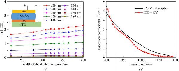
Fig.4 Estimation of diffusion length by the bias dependent IQE method. (a) −ln(1−IQE) against depletion width (x d). The diffusion length and absorption coefficient were extracted by the intercept and slope of the linear fitting. (b) Comparison between the absorption coefficient derived from IQE+ CV (red dots line) and the measured value from transmittance (black line) |
3.5 Defect depth
Temperature dependent dark conductivity was measured to investigate defect types and depths in our Sb2Se3 thin films with [221] orientation. We used a symmetric device structure, Au/Sb2Se3/Au, with glass as the substrates and Au electrodes with a spacing of 200 mm as the Ohmic contacts. I-V measurements in the temperature ranging from 85 to 420 K were performed on an Agilent B1500A in dark condition. A liquid nitrogen cryostat (Variable Temperature Insert Cryostat, CRYO Industries of America Inc.) was used to regulate the temperature. Resistances were evaluated around the zero-bias voltage from I-V data by linear least-square fitting.
The conductivity of Sb2Se3 film at 85 to 420 K was in the order of 10−4 to 10−11 S·cm−1 (see Fig. 5(a)). We identify two different transport mechanisms. At high temperatures (above 160 K), the electrical conductivity depends on the number of carriers thermally activated from the defects to the band, which again depend on defect depth and temperature, as shown in Eq. (6) [30]:
where E 1,2 is the activation energies and σ 1,2 is the pre-exponential factor, k B is Boltzmann constant and T is the absolute temperature. Two linear regions were observed in Fig. 5(a) (lnσ against 1000/T), and the corresponding activation energies were obtained by fitting Eq. (6). Between 250 and 420 K, the activation energy E 1 is (0.578±0.009) eV, which is approximately half of the direct band gap (1.17 eV) of Sb2Se3. In this temperature region, intrinsic excitation dominates the carrier density. Between 160 and 250 K, the fitted activation energy E 2 was (0.111±0.005) eV, corresponding to a defect depth of 0.111 eV. This defect is ascribed to the acceptor defect of SeSb as suggested by theoretical calculation that SeSb has the lowest formation energy and is a shallow acceptor with defect depth of approximately 0.1 eV [31]. In the low temperature region (85−160 K), the conductivity is slowly reduced with the temperature because the conduction mechanism change into Mott’s variable range hopping between localized states [32]. The conductivity as a function of temperature is described in Eq. (7):
where T0 is a characteristic temperature which is related to the disorder of the material, σ0' is a constant, and T is the absolute temperature. Figure 5(b) shows the plot of ln(σT1/2) against T−1/4. It is clear that the relation is linear, which indicates the occurrence of a hopping conduction mechanism and from which we can calculate the characteristic temperature T0 as 2.31 × 10⁶ K. This value is larger than the values of CZTS and CIGS [33], implying more disorder in our Sb2Se3 films.

3.6 Density of defect states
As discussed above, we believe shallow acceptor SeSb was the dominant defects in our Sb2Se3 films produced by RTE. Using the T. Walter’s method [34], we could extract the density of defect states from thermal admittance spectroscopy (TAS). Device configuration for TAS measurement was ITO/CdS/Sb2Se3/Au as the inset in Fig. 4(a), our standard superstrate solar cell configuration. The experiments were performed using Keithley 4200-CVU module with frequencies ranging from 1 kHz to 10 MHz. The energy profile of trap density of states (N t) can be derived from the angular frequency dependent capacitance according to Eq. (8) [34]:
where C is the capacitance, ω is the angular frequency (ω = 2πf), q is the elementary charge, k B is the Boltzmann constant and T is absolute temperature. V bi and x d are the built-in potential and depletion width, respectively, which were extracted from C-V measurement. The applied angular frequency ω defines an energetic demarcation as Eq. (9) [34]:
where E ω is the energy depth of the defect relative to the corresponding band edge, ω 0 is the attempt-to-escape frequency which is related to defect capture cross section, effective density of states in the valence band, and thermal velocity. Figure 6(a) is the density of defect states. There was a Gaussian defect peak in the gap with the peak position at (0.095±0.008) eV, which was consistent with the defect depth of (0.111±0.005) eV obtained from temperature dependent conductivity measurement. The profile of the defect distribution is shown in Fig. 6(b). The density of defect states was about 1016 cm−3·eV−1 at the peak position and the integrated defect density was 1.3 × 1015 cm−3.
The defect density could also be extracted from space charge limited current (SCLC) measurement [35] at the transition regime between the linear region and the quadratic region (as seen in supplemental material [24]). The trap density nt was 6.9 × 1014 cm−3 based on the SCLC result, in good agreement with the value obtained from TAS. We should emphasize that our first-principle calculation using VSAP code also predicted an equilibrium defect density of 1 × 1015 cm−3 for Sb2Se3 film at room temperature [31], thus validating our experimental results. Assuming the probability of defect activation dictated by the Fermi-Dirac distribution as 1/{1+ exp[(Et−EF)/kT]}, the activated percentage of defects would be 3.4% corresponding to the extremely low doping density of 2.4 × 1013 cm−3, echoing our previous carrier density measurement.

3.7 Optical band tail
Band tails in the optical absorption band edges are observed in many disorder materials. For photovoltaic applications, the local band tail state can lead to the degradation of device performance particularly for V OC. It can be caused by doping or disorder due to the destruction of the lattice periodicity. The band tail can be investigated by photothermal deflection spectroscopy (PDS), which is widely used to examine the optical properties of materials [19]. The devices for PDS measurement were prepared by depositing 1000 nm crystalline (c-Sb2Se3) films on quartz glass using RTE. PDS spectra were acquired from 0.6 to 2.5 eV, and were subsequently repeated over the course of several days. We found no appreciable change in the PDS signal, thus verifying the stability of these materials against the index fluid, perfluorohexane. The detailed test process is shown in supplemental material [24]. We obtained absorption coefficients by first system correcting the raw data using a “blackbody” spectrum from a graphite thin film painted on glass substrates identical to those used for sample growth. We then scaled the PDS spectra to make the above gap data consistent with absorptance, A = 1−R–T (R and T represent reflectance and transmittance, respectively), data that was obtained with a Cary 2500 and integrating sphere. Lastly we converted the absorptance to absorption coefficient (α) using Eq. (10), neglecting reflections from the film-substrate interface [36],
where d is the sample thickness. The PDS spectrum were shown in Fig. 7. The Urbach energy was estimated from fitting the exponential band-edge portion of the absorption coefficient versus energy plot by Eq. (11) [37].
where h n is the photon energy, U 0 is the Urbach energy, U 1, and α 0 are constants determined by fits to experiment. In the energy range of 1.1 to 1.25 eV, the Urbach energy is (38±3) meV. Another extremely large Urbach energy ((129±7) meV) was observed in lower energy region (0.8 to 1.1 eV) in the crystal Sb2Se3 spectra. This unusually large value may result not from the Sb2Se3 film, but from other non-stoichiometric phases in the film that occur during growth in non-optimal conditions. For example, the presence of oxygen during growth may consume antimony and leave selenium rich regions, which are more disordered. These observations (i.e. antimony oxides, etc.) help explain the low device performance for our Sb2Se3 solar cells, and motivate further optimization of growth conditions.
To test this speculation, we measured the PDS spectra of amorphous Sb2Se3 film (black dots in Fig. 7) which was completely disordered and then compared it to the crystalline counterparts (red dots in Fig. 7). A-Sb2Se3 film was deposited by thermal evaporation (TE) with the substrate kept at room temperature. The a-Sb2Se3 PDS spectra showed only one exponential region with Urbach energy (79±2) meV, while in the crystalline samples, the large Urbach energy region begins near 1 eV.

4 Discussion
The obtained physical properties of RTE deprived Sb2Se3 film are summarized in Table 1. We now discuss the cons and pros of our Sb2Se3 thin films in terms of optoelectronic properties, as well as the suggested strategies for further efficiency improvement based on our characterization.
Tab.1 Summary of physical parameters of Sb2Se3 reported in this paper |
| parameter | value | characterization method | |
|---|---|---|---|
| e r | 18 | CF, 2 MHz | |
| 29 | CF, 2 kHz | ||
| μ h/(cm2·V−1·s−1) | a | 1.17 | TOF |
| b | 0.69 | ||
| c | 2.59 | ||
| μ e/(cm2·V−1·s−1) | c | >16.9 | Hall effect |
| τ e/ns | 67±7 | TA | |
| L e/mm | [221] | 0.29±0.03 | bias IQE, low illumination |
| [001] | 1.7±0.2 | calculated, high illumination | |
| n t/cm−3 | 6.9 × 10¹⁴ | SCLC | |
| 1.3 × 10¹⁵ | TAS | ||
| (E t −E v)/eV | 0.095±0.008 | TAS | |
| E 1/eV | 0.578±0.009 | conductivity | |
| E 2/eV | 0.111±0.005 | conductivity | |
| T 0/K | 2.31 × 10⁶ | conductivity | |
| U 0/meV | c-Sb2Se3 | 38±3 | (1.1−1.25 eV) PDS |
| c-Sb2Se3 | 129±7 | (0.8−1.1 eV) PDS | |
| a-Sb2Se3 | 79±2 | (0.8−1.25 eV) PDS | |
First, we argue that pseudo-direct optical transition nature of Sb2Se3 might be beneficial for photovoltaic application. For our Sb2Se3, the lowest indirect band gap (E ind) is 1.04 eV and the lowest direct band gap (E d) is 1.17 eV at room temperature [3], which means Sb2Se3 absorption starts at 1192 nm and then changes to strong absorption at 1060 nm due to the p->p transition [38] and direct band gap. Presently, absorption is not a limiting factor, as J SC of 25 mA·cm−2 was obtained in our certified device with the Sb2Se3 absorber of only 390 nm thickness. One natural advantage of pseudo-direct band gap is the long carrier lifetime owning to the phonon-assisted recombination nature. The TA derived carrier lifetime is 67 ns, which is shorter than CH3NH3PbI3 (288 ns from TA measurement) [39] and the best CdTe single crystals (400 ns, single-photon counted decay) [40], but significantly longer than CZTSSe (6.7 ns measured from photoluminescence decay) [41], CIGS (5.5 ns measured from photoluminescence decay) [42] and SnS (<100 ps measured from transient terahertz photoconductivity) [43]. One further advantage associated with high absorption coefficient and long carrier lifetime is that Sb2Se3 can maintain high non-equilibrium carrier density under AM1.5G illumination, thus permitting large Fermi level splitting and higher open circuit voltages.
Second, we discuss the implication of the measured mobility of our Sb2Se3 film. The along-ribbon mobility of Sb2Se3 lies in 1−20 cm2·V−1·s−1, better than PbS CQDs (0.001−0.1 cm2·V−1·s−1) [44], Cs2SnI6 (2.9 cm2·V−1·s−1) [45] and CuZnSn(S,Se)4 (0.5−1.3 cm2·V−1·s−1) [46] yet worse than Bi2S3 (257 cm2·V−1·s−1) [47], CH3NH3PbI3 (15−40 cm2·V−1·s−1) [48] and SnS (128 cm2·V−1·s−1) [49]. Mediocre carrier mobility in combination with the better-than-average carrier lifetime results in a decent diffusion length approaching 1.7 mm under strong light illumination, which is much better than PbS CQDs solid which has strived for>300 nm diffusion length for years and now has obtained certified device efficiency of 10.7% [50]. The concern is the highly anisotropic nature of mobility due to its one-dimensional crystal structure. Stringent control of c-axis oriented film is imperial for high efficiency thin film solar cells, and preliminary success was obtained through deposition temperature control.
Last we would discuss the defects and doping density in Sb2Se3. Previous theoretical simulation, and the present experimental results included here suggest that the dominant defect in Sb2Se3 film produced by RTE strategy is SeSb acceptor with defect depth of ~0.1 eV and density of ~1 × 1015 cm−3. Defect depth is acceptable yet shallower defects such as V Cu in CIGS with a depth of ~0.03 eV is preferable. The doping density (~1013 cm−3) is far lower than the optimal value of approximately 1016 cm−3 for the absorber layer in a photovoltaic device. Whether this is intrinsic for this material, or it is because of the strong compensation by defect pairs remains elusive at this stage. Strategies to significantly increase carrier density in Sb2Se3 film deserve further efforts. Alternatively, construction of device with p-i-n configuration, in analogy to heterostructure with intrinsic thin layer (HIT) silicon or perovskite solar cell, would probably circumvent this obstacle. In addition, the large band tail in our Sb2Se3 films is harmful to solar cells. However, it may be overcome by supplementing Se element, increasing the crystallinity and eliminating the secondary phase such as Sb2O3.
5 Conclusion
In conclusion, we have systematically studied the photovoltaic relevant physical properties of Sb2Se3 film produced from RTE. The dielectric constant of Sb2Se3 is measured to be between 29 to 18 within the frequency 2 kHz−2 MHz. TOF measurements revealed that the hole mobility in a single Sb2Se3 grain along a-, b- and c-directions were 1.17, 0.69 and 2.59 cm2·V−1·s−2, respectively. Hall measurement at elevated temperature suggested that the electron mobility along c-direction was larger than 16.9 cm2·V−1·s−1. Fs-TA and ns-TA spectrum illustrated the non-equilibrium carrier dynamics upon photoexcitation, and the minority carrier lifetime was fitted as (67±7) ns based on TA characterization. The electron diffusion length along c-direction under high illumination was (1.7±0.2) mm, while under low illumination along the [221] direction was (0.29±0.03) mm. Temperature dependent dark conductivity measurement indicated two thermal activation energies of (0.578±0.009) eV and (0.111±0.005) eV, corresponding to intrinsic thermal excitation and defect activation, respectively. Admittance spectroscopy was used to determine the density of defect states in the order of 1016 cm−3·eV−1 and the position of defect peaked at (0.095±0.008) eV. The corresponding integrated defect density is 1.3 × 1015 cm−3 which is in good agreement with that of 6.9 × 1014 cm−3 obtained from SCLC. The free carrier density was about 1.8 × 1013 cm−3. The Urbach energy of c-Sb2Se3 is (38±3) meV in the range of 1.1 to 1.25 eV and (129±7) meV in the range of 0.8 to 1.1 eV, while the Urbach energy of a-Sb2Se3 is (79±2) meV in the range of 0.8 to 1.25 eV. The reasonably good optoelectronic properties revealed here, coupled with its excellent material properties such as simple and stable phase, non-toxic and low-cost constituents, rendering our Sb2Se3 stands out among many emerging absorber materials and thus deserving further extensive study.